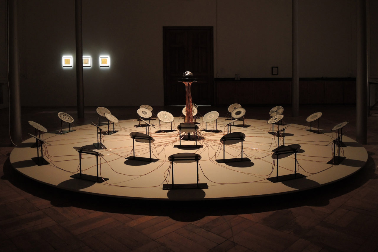
The Power of None (2018), Artefact, STUK, Leuven, Belgium, 2018 (photo: Kristof Vrancken)

The Power of None (2018), Artefact, STUK, Leuven, Belgium, 2018 (photo: Kristof Vrancken)
'The Power of None' is a multifaceted installation that deals with the different agencies of silicon, tracing its past, present and future potential. It is the basic material in the production of integrated circuits used in computers, TVs, mobile phones and all types of electronic equipment and semiconductor devices, and is also used in large quantities for the production of photovoltaic solar cells. Since the beginning of the digital revolution, microchips made of silicon have consistently been reducing in size, as articulated in Moore’s Law in 1965 (Intel founder Gordon E. Moore predicted that the number of transistors on a microchip would double every two years, though the cost of computers has halved). By the beginning of the twenty-first century the traditional chip circuitry made of silicon had become too microscopic to work reliably, marking the end of the silicon age.
In the centre of 'The Power of None' is a silicon copy of a human brain, commemorating humans as the first computers, or ‘calculators’ as they were called in the mid-twentieth century. Surrounding it is a field of silicon wafers – the raw material used to produce transistors – mounted on supports such as circular solar panels and connected to the central brain by raw copper wires, arranged to resemble a devoted army or cult. Made visible on the silicon wafers is a variety of centric diatoms. Diatoms form a major group of micro-algae and are one of the commonest types of phytoplankton; uniquely, their cell wall is made of silica. Researchers use diatoms and other single-celled algae as templates for developing new solar cells that can produce up to three times as much energy as conventional ones.
The diatoms in 'The Power of None' are derived from the world-famous 'Universum Diatomacearum Möllerianum', which is housed in a vault in the Meise Botanic Garden in Belgium. Made by Johann Diedrich Möller in 1890 and consisting of 4026 different species of diatom, it is the micro- biologists’ holy grail. The original images of the individual diatoms, each with a unique ornamental form, are scanned and transferred onto the silicon wafers using specialised photography and printing techniques.